| Index | wersja polska |
| Pin | Symbol | Function |
|---|---|---|
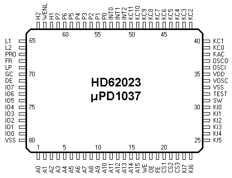
| 1..16 | A0..A15 | address bus |
| 17 | WE | bus write strobe signal, active low |
| 18 | OE | bus read strobe signal, active low |
| 19..22 | FE, CS1..CS3 | chip enable signals, active low FE: ROM 32kB CS3: RAM 8kB |
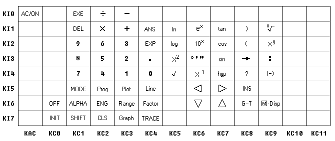
| 23..30 | KI7..KI0 | keyboard matrix input port, can be accessed through the KY register |
| 31 | SW | |
| 32 | TEST | |
| 33 | VSS | negative supply voltage rail |
| 34 | VOSC | Power supply for Clock |
| 35 | VDD | positive supply voltage rail |
| 36,37 | OSCI, OSCO | ceramic resonator 2.01MHz, OSCO is the output from the inverting oscillator amplifier |
| 38..50 | KAC, KC0..KC11 | keyboard matrix output port, controlled by the KY register |
| 51..53 | INT2..INT0 | interrupt inputs, unused, connected to VSS |
| 54..61 | P0..P7 | 8-bit bi-directional port, can be accessed through the PD register Function of individual bits: |
| 62 | H1 | 4-bit output port, controlled through the PE register |
| 63 | WENL | connected to VSS |
| 64..66 | H2, L1, L2 | 4-bit output port, controlled through the PE register |
| 67 68 69 70 71 | PRO FR LP GC DE |
LCD driver control signals |
| 72..79 | IO7..IO0 | bi-directional data bus |
| 80 | VSS | negative supply voltage rail |
The columns of the keyboard matrix are driven from the 13-bit output port KC. A pressed key makes contact between selected column and row. The rows are sensed by the 8-bit input port KI.