| Index | wersja polska |
[click on the picture to enlarge]
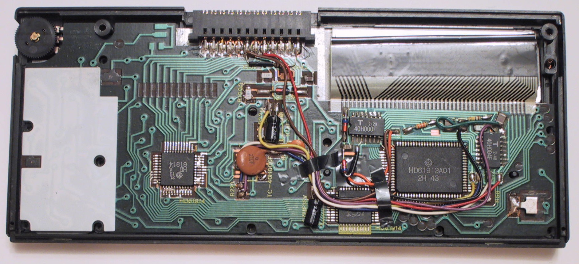
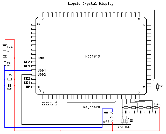
The FX-700P uses a microprocessor HD61913A01 with internal program ROM, built in LCD driver and keyboard controller. The microprocessor can communicate with external data memory and peripherals through a bi-directional 4-bit bus.
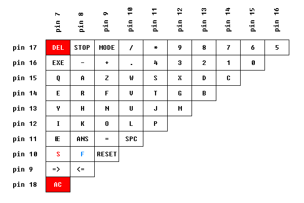
Usually the keyboard port pins are separated in two groups: rows configured as outputs, and columns configured as inputs.
A pressed key makes contact between selected row and column.
However, in the Casio FX-700P there isn't any ordinary key matrix with rows and columns, but a key can be connected between any pair of pins.
Such layout needs less port pins for a specified number of keys at the cost of more complex key scan algorithm.
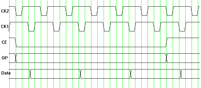
The Data lines are bi-directional with weak pull-ups.
Negative logic on the Data lines applies, i.e. high level is assumed as logical 0, while low level as logical 1.
CE (Chip Enable) line - active low.
OP line selects data transfer to the Command Register (OP=0, write only) or Data Register (OP=1, read/write).
This signal shouldn't change when the CE line is low.
All system bus lines can be tri-stated which allows external access to the RAM.
The CK1, CK2 frequency is ca. 200kHz.
The FX-700P contains two memory chips HD61914A occupying data address space $0000-$07FF and $0800-$0FFF respectively. A similar model PB-100 comes with only single memory chip on board, which can be expanded by adding a second one inside the optional OR-1 memory pack. Further memory expansion isn't supported by the BASIC interpreter.
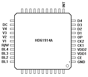
| Pin | Function |
|---|---|
| D4-D1 | bi-directional data bus |
| OP | register select |
| CK1, CK2 | bi-phase clock |
| CE | Chip Enable, active low |
| V1 | Device Address Select, bit A11 |
| GND | positive supply voltage rail |
| VDD2 | -5V when operational, 0V when stand-by |
| VDD1 | connected to -5V through a 390ohm resistor |
Pins 24-27 and 29-33 are connected to GND in the calculator. Some of them (i.e. V2-V4) may function as additional address select lines (A12-A14), but I haven't tested this. All other pins aren't connected.
| Code | Function | Description |
|---|---|---|
| $4 | Write | The Write command (OP=0) consists of a 4-bit word $4, followed by three 4-bit words containing the 11-bit address within the device (the least significant word first), and a 4-bit word containing the Device Address. The most significant bit of the address within the device is ignored. After issuing this command any amount of data can be written to the memory (in an OP=1 cycle). The address counter advances after each transmitted 4-bit word. |
| $0 | Read | The Read command is similar to Write, except that the first 4-bit word contains $0 instead of $4.
After issuing this command any amount of data can be read from the memory (in an OP=1 cycle).
The address counter advances after each transmitted 4-bit word. A single 4-bit word $0 regularly appears on the bus when the calculator is idle. I don't know its exact purpose, probably a sort of reset. |
    OP=0 40C71          ;write to address $0FC0
    OP=1 12A            ;data written: $0FC0<-$1, $0FC1<-$2, $0FC2<-$A

    OP=0 04630		;read from address $0364
    OP=1 7C		;data read: $0364->$7, $0365->$C

    OP=0 0              ;reset
| Expansion Port Pin |
Processor Pin |
Symbol | Function |
|---|---|---|---|
| 1 | 4 | D4 | Data 4 |
| 2 | 3 | D3 | Data 3 |
| 3 | 2 | D2 | Data 2 |
| 4 | 1 | D1 | Data 1 |
| 5 | 80 | OP | register select |
| 6 | 79 | CK2 | bi-phase clock |
| 7 | 78 | CK1 | bi-phase clock |
| 8 | 77* | VDD3 | -5V when operational, 0V when stand-by |
| 9 | 75 | CE1 | RAM Chip Enable, active low |
| 10 | 74 | CE2 | Cassette Interface Chip Enable, active low |
| 11 | 76 | VDD1 | negative supply voltage rail |
| 12 | 73 | GND | positive supply voltage rail |
An asterisk means that the microprocessor's pin is connected to the bus not directly, but through additional circuit.
Only small current of few mA can be drawn from the power terminals. More would cause too much voltage drop, as the internal voltage regulator consists only of a silicon diode and a 100ohm resistor in series.
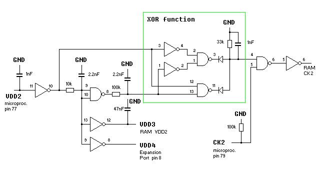
The schematic below shows the circuit on an additional PCB mounted near the microprocessor. Presumably it should prevent RAM data corruption while switching the unit on/off. Any on/stand-by signal change causes a short pulse on the XOR gate output disabling the RAM CK2 signal for a while.
The cassette interface is selected when the CE2 line goes low. It exchanges information through the Data4 line only (note the inverted logic convention on the Data lines).
| Code | Function | Description |
|---|---|---|
| 101000 | Open for write | This command opens the communication channel for write. |
| 011000 | Open for read | This command opens the communication channel for read. |
| 000100 | Read status | The calculator issues this command with OP=0, then reads a single data bit with OP=1. Returned value=0 means the cassette interface is busy or absent, while 1 means it's ready to accept/send data. ERR9 when timed out. |
| 010010 | Transfer data | The calculator issues this command with OP=0, then sends the data byte serially in an OP=1 cycle in the following order:
Before sending any actual data, a leader signal consisting of ca. 160 words of 111111111111xxxx needs to be written (to settle things like tape speed, record level etc.). |
| 100100 | Carrier detected | The calcualator issues this command in the LOAD mode after correct reception of the first 12 leader signal words. From now on, data sent from the interface to the calculator are synchronized by the start pulse. |
| 000000 | Reset | This command closes the communication channel. |
| 111100 | Close | Usually the calculator terminates the transfer with the Reset command. However, the transfer initiated by the LOAD statement is terminated with this Close command. GET still uses Reset at this place. |
    Tape write
    ==========

1.  OP=0 101000         ;open the communication channel for write

2.  OP=0 000100         ;repeat this sequence, until the interface
    OP=1 0 or 1         ;returns 1

    OP=0 010010         ;write a word of the leader signal
    OP=1 1111111111111111

3.  goto 2, until ca. 160 words written

4.  OP=0 000100         ;repeat this sequence, until the interface
    OP=1 0 or 1         ;returns 1

    OP=0 010010         ;write the data byte ($63 in this example)
    OP=1 0110001100111111

5.  goto 4, until all data written

6.  OP=0 000000         ;reset, close the communication channel

    Tape read
    =========

1.  OP=0 011000         ;open the communication channel for read

2.  OP=0 000100         ;repeat this sequence, until the interface
    OP=1 0 or 1         ;returns 1

    OP=0 010010         ;read a word of the leader signal
    OP=1 1111111111111111

3.  goto 2, until 12 words read

4.  OP=0 100100		;issue the "carrier detected" command

5.  OP=0 000100         ;repeat this sequence, until the interface
    OP=1 0 or 1         ;returns 1

    OP=0 010010         ;read data
    OP=1 1111010010011011 ;data = $C9 in this example

6.  goto 5, until all data read

7.  OP=0 000000         ;reset, close the communication channel
The printer interface uses the RAM locations $0132-$0133 for data transfer.
The communication protocol also uses control commands consisting of a 4-bit word transmitted at OP=0, followed by the same 4-bit word transmitted at OP=1.
Both words transmitted with CE1=1 and CE2=1.
| Code | Function |
|---|---|
| $80 | inserted between the expression and result in the calculator mode, printed as a space |
| $F0 | appended after each listed BASIC line, seems to be ignored by the printer |
| $FD | the calculator emits this code when the AC key is pressed, cancels printing and flushes the printer's buffer |
| $FE | used as a separator between actual characters |
| $FF | carriage return/line feed |