| Index | wersja polska |
On this page only information specific to the FX-870P is shown. See the PB-1000 hardware page for more general information about the microprocessor and the bus waveforms.
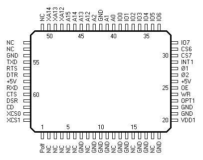
CS0: &H00C00..&H0FFFF and &H20000..&H2FFFF, ROM 128kB
CS1: &H34000..&H37FFF, unused
CS2: &H30000..&H30001, unused
CS3: &H38000..&H3FFFF, peripheral port
CS4: &H32000..&H33FFF, unused
CS5: &H31000..&H31FFF, unused
CS6: &H10000..&H1FFFF, gate array (RAM address space)
CS7: &H30000..&H30007, gate array (registers)
P7..P6 drive the piezo-buzzer
P5 is the printer port BUSY input
P4 selects the language version, connected either through the PAD3 jumper to +5V (Japanese) or through the PAD4 jumper to GND (some unreleased export version)
P3 is the printer port STROBE output
P2 is the printer port INIT output
P1 is not connected
P0 receives high level from the S8054ALR battery monitor chip when valid supply voltage is present
The clock signals Ø1 and Ø2 are distributed to the peripheral devices through a loading coil.
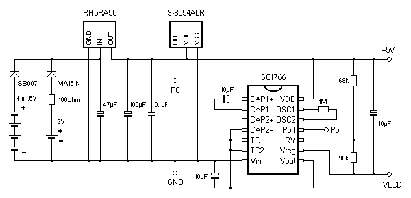
Unlike the PB-1000 and PB-2000C, the FX-870P uses the negative supply voltage rail as ground (GND).
| Pin | Symbol | Function |
|---|---|---|
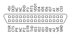
| 1 | Poff | controls the Poff input of the voltage converter chip SCI7661 |
| 20 | VDD1 | receives low level from the microprocessor pin 33 when the power is on |
| 23 | OPT1 | selects the RAM configuration, connected either through the PAD1 jumper to +5V (8kB RAM soldered on the board) or through the PAD2 jumper to GND (32 kB RAM soldered on the board) |
| 24 | WR | bus write strobe signal, active low |
| 25 | OE | data strobe control signal |
| 27 28 | Ø2 Ø1 |
bi-phase clock signal from the microprocessor |
| 29 | INT1 | interrupt request output, active low |
| 30 | CS7 | chip enable input for the gate array registers, receives low level from the microprocessor for address range &H30000..&H30007 |
| 31 | CS6 | chip enable input for the RAM address space, receives low level from the microprocessor for address range &H10000..&H1FFFF |
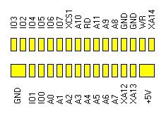
| 32..39 | IO7..IO0 | bi-directional data bus |
| 40..41 | A0, A1 | address bus inputs |
| 43..47 | A2, A12..A15 | address bus inputs |
| 48..50 | XA12..XA14 | address bus outputs for the RAM, the same state as A12..A14 when the OPT1 input is high, or after subtracting an offset of &H3000 from the address sent by the microprocessor when the OPT1 input is low This address translation is redundant, the system would work just as well with the RAM connected directly to the microprocessor address bus. |
| 55 | TXD | serial port transmit data output |
| 56 57 | RTS DTR |
serial port control signals |
| 59 | RXD | serial port receive data input |
| 60 61 62 | CTS DSR CD |
serial port status signals |
| 63 | XCS0 | chip enable output for the RAM soldered on the board, decoded address range &H11000..&H12FFF when the OPT1 input is high, or &H10000..&H17FFF when the OPT1 input is low |
| 64 | XCS1 | chip enable output for the RAM expansion module, decoded address range &H13000..&H1AFFF when the OPT1 input is high, or &H18000..&H1FFFF when the OPT1 input is low |
| A2 | A1 | A0 | Access | Function |
|---|---|---|---|---|
| 0 | 1 | 0 | Read | serial port receive data register |
| Write | serial port transmit data register | |||
| 0 | 1 | 1 | Read | bit 0 - set when the transmitter is ready for data to be sent bit 1 - flag of a received byte, cleared after reading data register 010 bit 2 bit 3 - set by a parity error bit 4 - set by an overrun error bit 5 - set by a framing error |
| Write | bit 0 bit 1 bit 2 - set when 8 data bits, cleared when 7 data bits bit 3 bit 4 - set turns the parity control on bit 5 - set when parity even, cleared when parity odd bit 6 - set for this function bit 7 - set when 2 stop bits, cleared when 1 stop bit | |||
| bit 0 bit 1 - state of the RTS output (inverted) bit 2 bit 3 bit 4 bit 5 - state of the DTR output (inverted) bit 6 - cleared for this function bit 7 | ||||
| 1 | 0 | 0 | Read/Write | bit 0..2 - baud rate for RS232C transfer and MT writing bit 3 bit 4 bit 5 - set when reading from MT in Slow mode, cleared when in Fast mode bit 6 - receiver enable bit 7 - transmitter enable |
| 1 | 0 | 1 | Read/Write | bit 2 - set when MT, cleared when RS232C bit 4 - inversion of the loaded MT signal |
| 1 | 1 | 0 | Read | bit 0 - set on valid carrier tone from the tape bit 2 - state of the CTS input (inverted) bit 3 - state of the DSR input (inverted) bit 4 - state of the DCD input (inverted) bit 7 - state of the OPT1 input |
| Write | ||||
| 1 | 1 | 1 | Read/Write |
| bits 210 |
baud rate |
|---|---|
| 001 | 4800 |
| 010 | 2400 |
| 011 | 1200 |
| 100 | 600 |
| 101 | 300 |
| 110 | 150 |
01 - GND 02 - +5V 03 - VLCD 04 - ON 05 - Ø1 06 - Ø2 07 - OP 08 - CE1 09 - CE2 10 - VDD2 11 - D0 12 - D1 13 - D2 14 - D3 15 - GND |
01 - GND 02 - KI12 03 - KI11 04 - KI10 05 - KI9 06 - KI8 07 - KI7 08 - KI6 09 - KI5 10 - KI4 11 - KI3 12 - KO1 13 - KO2 14 - KO3 15 - KO4 16 - KO5 17 - KO6 18 - KO7 19 - KO8 20 - KO9 |
The columns of the keyboard matrix are driven from the 12-bit KO output port, controlled by the IA register. A pressed key makes contact between selected column and row. The rows are sensed by the 12-bit KI input port, accessible through the KY register.
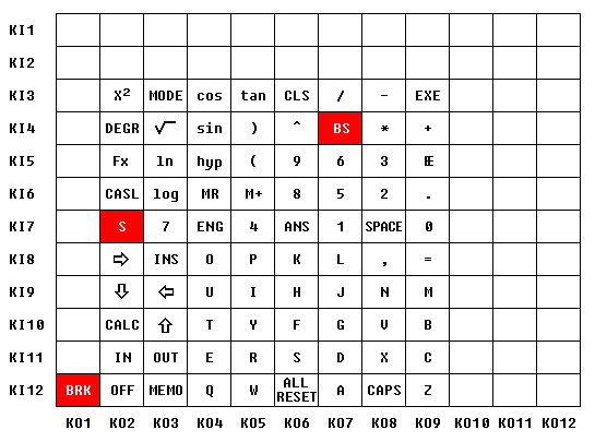
Mapping of the KY register bits to the keyboard rows:
![]()