| Index | wersja polska |
Signal naming according to the "PB-1000 technical handbook" published by the MODERN CO, LTD, Japan.
Credits to BLUE for his great help.
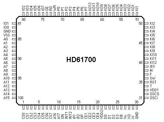
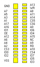
| Pin | Symbol | Function |
|---|---|---|
| 1..8 | CS0..CS7 | Chip select signals, active low.
Following address ranges are decoded: CS0: &H08000..&H0FFFF, ROM 32kB CS1: &H04000..&H05FFF, goes to the expansion port, unused CS2: &H06000..&H07FFF, internal RAM 8kB CS3: &H18000..&H19FFF, additional RAM module CS4: &H1A000..&H1BFFF, additional RAM module CS5: &H1C000..&H1DFFF, additional RAM module CS6: &H1E000..&H1FFFF, additional RAM module CS7: &H00C00..&H00C0F, serial, printer and FDD interface |
| 9,10 | A16,A17 | two most significant bits of the address bus |
| 11 | ON | ON interrupt request input, receives low level pulses of frequency 55 Hz from pin 27 of the HD44352 LCD controller chip, the handler routine starts at address &HFFCA |
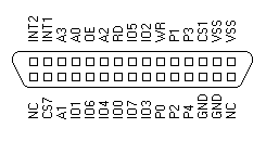
| 12 | INT1 | edge sensitive interrupt request input, connected to the peripheral port, the handler routine starts at address &HFFBB |
| 13 | INT2 | level sensitive interrupt request input, connected to the peripheral port, the handler routine starts at address &HFFD0 |
| 14..25 | Ø1,Ø2 OP CE1..CE4 VDD2 D0..D3 |
LCD controller bus, similar as in the Casio FX-700P, all signals use negative logic, pins CE3 and CE4 are not connected in the Casio PB-1000 |
| 26 | DB | jumper E to VSS (open), low level selects debug mode |
| 27 | Vx | filter capacitor 0.47uF for the 32768Hz oscillator supply voltage |
| 28,29 | XO,XI | crystal 32768Hz, XO is the output from the inverting oscillator amplifier |
| 30 | GND | connected to GND |
| 31,32 | OSCI,OSCO | ceramic resonator 910kHz, OSCO is the output from the inverting oscillator amplifier |
| 33 | VDD1 | internal logic power supply, outputs low level when the power is on, controls the Poff input of the voltage converter chip SCI7661 (through an inverter built with a pnp transistor) |
| 34 | T | connected either to GND through the jumper A (soldered) or to VSS through the jumper C (open), low level selects the test mode |
| 35 | RST | Reset input, active low, pressing the RESET button connects this pin to VSS |
| 36 | SW | Power on interrupt request input, connected by the Power switch either to VSS (power on) or to GND (power off), the handler routine starts at address &HFFC1 |
| 37 | F | this output informs whether the clock is divided by 16 high level: slow mode, low level: fast mode (opposite to the description in the "technical handbook") |
| 38 | M | operation code fetch signal in the debug mode |
| 39 | Ø3 | bus reading signal in the debug mode |
| 40..51 | KI1..KI12 | keyboard matrix input port, can be accessed through the KY register KI5 can be optionally connected to VSS through the jumper B (open), purpose unknown |
| 52..63 | KO1..KO12 | keyboard matrix output port, controlled by the IA register |
| 64..71 | P7..P0 | The 8-bit bi-directional port which can be accessed through the PD and PE registers.
Function of individual bits: P7,P6 drive the piezo-buzzer P5 senses the supply voltage P4 is the reset output for peripherals P3 controls the FDD power, 0 turns the power on P2 selects the FDD transfer direction, 1 when writing to the FDD interface, 0 when reading from the FDD interface P1 is connected to the expansion port, but not used P0 is the FDD transfer direction acknowledge input |
| 72 | WR | bus write strobe signal, active low |
| 73 | RD | bus read strobe signal, active low |
| 74 | OE | output enable for external memory, looks like the Motorola scheme data strobe control signal E, not used in the PB-1000 (except perhaps by some external peripherals) |
| 75..82 | IO7..IO0 | bi-directional data bus |
| 83 | GND | positive supply voltage rail |
| 84 | VSS | negative supply voltage rail |
| 85..100 | A0..A15 | address bus |
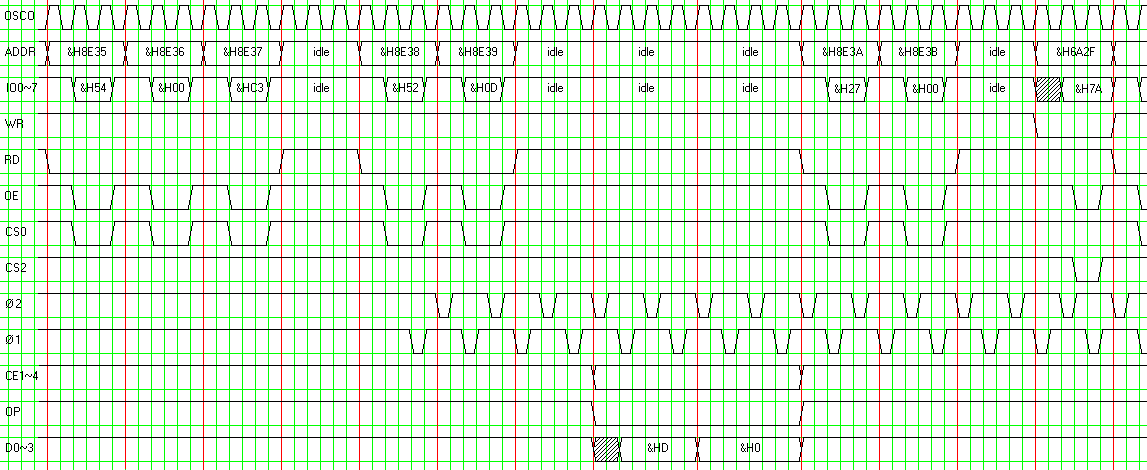
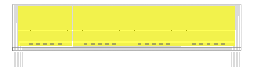
The diagram illustrates the system bus and the LCD port waveforms taken while executing following program:
8E35: 54 00 C3    PPO &HC3
8E38: 52 0D       STL &H0D ;data &H0D is transferred in two cycles,
                           ;the least significant nibble first
8E3A: 27 00       PHU $0   ;data &H7A written to address &H6A2F
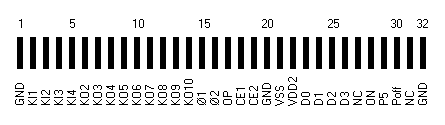
The columns of the keyboard matrix are driven from the 12-bit KO output port, controlled by the IA register. A pressed key makes contact between selected column and row. The rows are sensed by the 12-bit KI input port, accessible through the KY register.
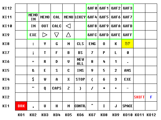
Mapping of the KY register bits to the keyboard rows:
![]()
GND is the positive terminal of the supply voltage, VSS is the negative terminal.
GND is the positive terminal of the supply voltage, VSS is the negative terminal.
Images contributed by Mahmoud Yassine.