| Index | wersja polska |
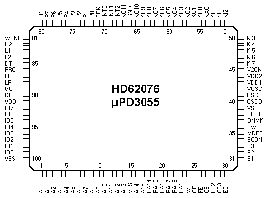
| Pin | Symbol | Function |
|---|---|---|
| 1..14 | A0..A13 | address bus |
| 15 | VSS | negative supply voltage rail |
| 16..17 | A14..A15 | address bus |
| 18..23 | RA14..RA19 | address bus |
| 24 | WE | bus write strobe signal, active low |
| 25 | OE | bus read strobe signal, active low |
| 26..29 | FE, CS1..CS3 | chip enable signals, active low CS3: RAM 64kB |
| 30..33 | E0..E3 | Chip enable signals, active low. E0: internal ROM 128kB E2: memory card, pin 20 E3: memory card, pin 33 |
| 34 | BCON | |
| 35 | MDP2 | |
| 36 | SW | |
| 37 | ONMK | |
| 38 | TEST | |
| 39 | VSS | negative supply voltage rail |
| 40,41 | OSCO, OSCI | ceramic resonator 2.01MHz, OSCO is the output from the inverting oscillator amplifier |
| 42 | VOSC | Power supply for Clock |
| 43,44 | VDD1, VDD2 | positive supply voltage rail |
| 45 | V2ON | Power on output signal |
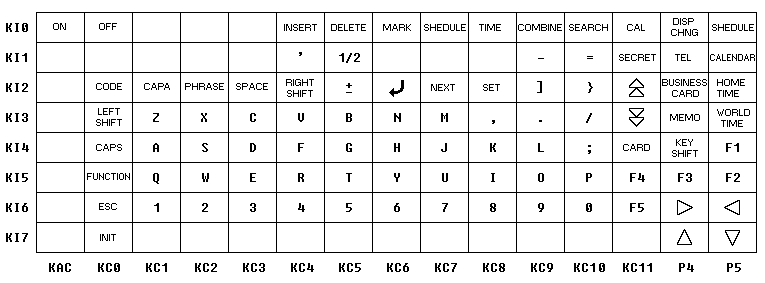
| 46..53 | KI7..KI0 | keyboard matrix input port, can be accessed through the KY register |
| 54..65 | KAC, KC0..KC10 | keyboard matrix output port, controlled by the KY register |
| 66 | GND | negative supply voltage rail |
| 67 | KC11 | keyboard matrix output port, controlled by the KY register |
| 68 | INT2 | interrupt input, driven from pin 28 of the chip HD62063 |
| 69 | INT1 | interrupt input, connected to P01 (serial data input) |
| 70 | INT0 | interrupt input, connected to P02 (state of the power switch) |
| 71 | BRK | |
| 72..79 | P0..P7 | 8-bit bi-directional port, can be accessed through the PD register Function of individual bits: P1 receives serial data from the communication port P2 receives high voltage level when the power switch is in the ON position, driven from pin 14 of the gate array μPD65005 P3 senses the card presence (low voltage level when a card is inserted) P4,P5 drive two lines of the keyboard matrix |
| 80 | H1 | 4-bit output port, controlled through the PE register |
| 81 | WENL | connected to VSS |
| 82..84 | H2, L1, L2 | 4-bit output port, controlled through the PE register L1: memory card, pin 32 (high voltage level enables access to the RAM inside the card) |
| 85 86 87 88 89 90 | DT PRO FR LP GC DE |
LCD driver control signals |
| 91 | VDD1 | positive supply voltage rail |
| 92..99 | IO7..IO0 | bi-directional data bus |
| 100 | VSS | negative supply voltage rail |
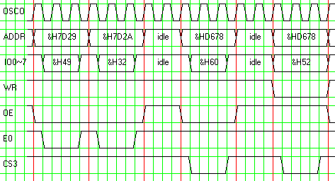
The diagram illustrates the system bus waveforms taken while executing following instruction:
7D29: 49 32 XR (IX),&H32
The columns of the keyboard matrix are driven from the 13-bit output port KC and two lines of the 8-bit port P0. A pressed key makes contact between selected column and row. The rows are sensed by the 8-bit input port KI.
  01 - VSS        16 - IO5        31 - A17
  02 - A12        17 - IO6        32 - L1
  03 - A7         18 - IO7        33 - E3
  04 - A6         19 - VCC        34 - A18
  05 - A5         20 - E2         35 - A19
  06 - A4         21 - A10        36 - IO0
  07 - A3         22 - RD         37 - IO1
  08 - A2         23 - A11        38 - IO2
  09 - A1         24 - A9         39 - IO3
  10 - A0         25 - A8         40 - IO4
  11 - IO0        26 - A13        41 - IO5
  12 - IO1        27 - WR         42 - IO6
  13 - IO2        28 - A14        43 - IO7
  14 - IO3        29 - A15        44 - P03
  15 - IO4        30 - A16        45 - VDD
pin 19 - VCC, supply voltage when the organizer is turned on
pins 36..43 - duplicate the function of pins 11..18
pin 44 - microprocessor port P3, senses the card presence, connected to VSS inside the card
pin 45 - VDD, backup supply voltage